By K.W. Current, K. Yuk, C. McConaghy, P.R.C. Gasoyne, J.A. Schwartz, J.V. Vykoukal, C. Andrews
Originally Appears: International Conference on MEMS, NANO and Smart Systems, 2005. pp. 153-158, Jul. 2005.
Abstract
A high-voltage (HV) integrated circuit has been demonstrated to transport droplets on programmable paths across its coated surface. This chip is the engine for a dielectrophoresis (DEP)-based micro-fluidic lab-on-a-chip system. This chip creates DEP forces that move and help inject droplets. Electrode excitation voltage and frequency are variable. With the electrodes driven with a 100V peak-to-peak periodic waveform, the maximum high-voltage electrode waveform frequency is about 200Hz. Data communication rate is variable up to 250kHz. This demonstration chip has a 32×32 array of nominally 100V electrode drivers. It is fabricated in a 130V SOI CMOS fabrication technology, dissipates a maximum of 1.87W, and is about 10.4 mm x 8.2 mm.
Introduction
Droplet-based programmable microfluidic processors promise to offer solutions to a wide range of applications in which chemical and biological analysis and/or small-scale synthesis are required. Such devices will become the microfluidic equivalents of electronic microprocessors by offering off-the-shelf solutions for almost any fluid-based analysis or synthesis problem. A general-purpose droplet processor should be able to manipulate droplets of different compositions (including those that are electrically conductive or insulating and those of polar or non-polar nature), to control reagent titrations accurately, and to remain free of contamination and carry over on its reaction surfaces. The programmable fluidic processor (PFP), a fluidic analog of a microprocessor, has a program memory that defines the movement of droplets or biological cells around the channel-less array of identical electrodes on the chip surface. Samples of various droplet sizes are accommodated and may be injected onto the chip surface above the electrode array from MEMS sample chambers to react with reagents or other chemicals. The electrode voltage excitation creates forces by employing dielectrophoresis (DEP) to move the sample and reagent droplets along arbitrary programmable paths across the electrode array [1]. These multiple droplets are moved simultaneously to the same array location and combined, forming a chemical reaction indicative of characteristics of the original chemical or biological sample. The resultant droplet is moved by DEP to a location for characterization. Motion and reaction results are now sensed optically. On-chip electronic location and characteristic sensing are in development. Low-voltage lab-on-a-chip devices employing DEP on planar microelectrode arrays have been reported in recent years [2, 3, 4]. The PFP can use both low-voltage and high-voltage excitations for droplet manipulation on a channel-less electrode array.
The PFP is programmable in several senses. Since the volumes and masses of various size biological cells and chemical molecules require various DEP forces to be moved, the PFP can accommodate them by having variable electrode excitation voltage amplitude, phase, and frequency. The path taken by each droplet on the array, the rate of movement across the chip surface, and the loading speed of the array memory are all variable, allowing complete flexibility for multiple reactions in chemical and biological fluid analyses.
Some advantages that this micro-scale PFP analyzer provides are the wider availability of valuable diagnostic tools; cheap, disposable units; reduced costs of chemicals and samples due to volume scaling; and versatility by testing multiple agents with a generic PFP analyzer type. Determination of chemical and cell characteristics using μL volumes, such as the sorting of cancer cells by electronic means has been demonstrated [5].
The electrode excitation chip is the engine for the programmable fluidic processor system summarized below. The chip architecture is an expandable NxN electrode array. The 10,377μm x 8210μm demonstration chip has a 32×32 electrode array. Electrode excitation amplitude, phase, and frequency are all variable up to limits. Using a 100V excitation voltage, the electrode excitation frequency can be up to 200Hz. Data communication rate using standard 5V CMOS logic signals is variable up to 250kHz. The 1024-element array of nominally 100V electrode drivers dissipates a maximum of 1.87W.
Dielectrophoresis
DEP forces can induce movement of uncharged but polarizable particles under the influence of an inhomogeneous electric field [6]. In positive DEP, a polarizable particle within a non- or less polarizable medium is polarized in the direction of an applied inhomogeneous electric field, creating a greater net force and movement towards the higher electric field gradient. In negative DEP, the particle is non- or less polarizable than its surrounding medium, causing the particle to be pushed away from the higher electric field gradient.
DC electric fields can be used to generate DEP forces, but AC electric fields are preferred to exploit the frequency-dependent dielectric properties of cells. The polarization direction of the particle’s charges exhibits an AC behavior when subject to an AC electric field. However, the resulting force can vary depending on the frequency and dielectric properties of the particle. The time averaged DEP force experienced by a particle can be expressed by

where εm is the permittivity of the medium, a is the radius of the particle, Erms is the electric field and Ke is the Claussius Mosotti factor, representing the complex permittivities of the particle [1,3,4]. The contribution of the complex permittivities of the particle, εp*, and of the medium, εm*, are contained in Ke, which can be expressed by

where

and

where ε is the permittivity and σ is the conductivity of the particle or suspending medium, and ω is the applied AC frequency. Therefore, the DEP force experienced by the particle and thus its movement in response to that force is a function of the frequency dependent dielectric properties of the particle and the medium and can be used for particle characterization and identification as well as manipulation [1, 5].
Programmable Fluidic Processor System
The block diagram of the entire Programmable Fluidic Processor (PFP) system and its support is shown in Figure 1. Indicated in the left hand side of the diagram is an Assay Development Host Computer that runs a user interface designed to create a sequence of commands that will be implemented by a personal digital assistant (PDA) and the electrode excitation integrated circuit (IC) engine described later. The assay development software gathers information about the fluids that will be in the sample and reagent chambers, the quantities of the fluids to be moved and combined, the time sequence of movements by the fluid droplets, sequence of combining of fluids, droplet movement to the optical sensors, droplet movement to the waste chambers, and other information necessary to control the PFP. Assay design templates help the user stay within practical timing, droplet volume, and other limitations inherent in the micro-fluidic system hardware. Multiple parallel injection operations and simultaneous multiple droplet movements are easily accommodated. The software prevents droplet collisions, but overlapping droplet locations may be forced when it is desired to combine droplets. Figure 2 illustrates a graphical droplet routing window used to design droplet movement on the PFP electrode array. Here a sequence of three sample droplets and three different reagents are injected from the left onto the reaction surface, combined, and exited from the right. The simulation of droplet behavior during the entire assay time or at any given instant can be viewed. The completed assay procedure is then compiled into commands that will be implemented by PFP software that runs in the PFP PDA controller. The compiled PDA commands for the entire assay are then transferred to the PDA as indicated in Figure 1. The PDA then controls the PFP at each step of the assay.
In Figure 1, the block labeled “Programmable Dielectrophoretic Array” is the high-voltage electrode driver IC engine to be described later. The top surface of the IC is the reaction surface for the system. The IC is mounted in a micro-fluidic MEMS structure that has several fluid reservoirs, and their corresponding channels that lead fluids to the reaction surface. A single type of electrode driver IC engine can be used with different organizations of the MEMS fluid structures. A variety of techniques may be used to help control fluid injection and drop size, and at present, optical sensing of droplet location and reaction results is used in flexible configurations. Electronic droplet location and reaction results sensing are now in development. The blocks within the PFP area of Figure 1 indicate a typical implementation of the MEMS structure. Variations are easily introduced.
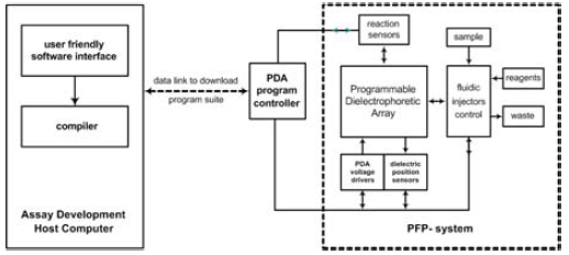
Figure 1. Architecture of an analysis instrument based on a Programmable Fluidic Processor (PFP). Droplets of samples and reagents are formed on the PFP and moved, merged, and measured under software control.
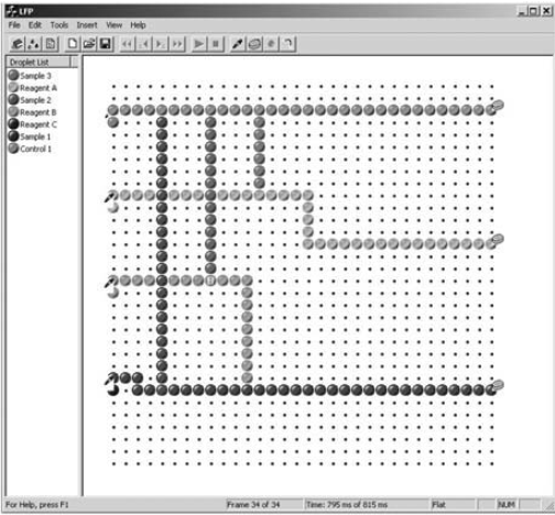
Figure 2. A routing diagram for a multi-droplet assay. Graphical design of droplet tracks and timing are easily generated using the assay development software.
The PFP electrode driver chip and MEMS structure cross-section is illustrated in Figure 3 [1]. The MEMS structure holds the fluid reservoirs and the fluid microchannels, and seals the edges of its reaction chamber (the open area of the MEMS structure directly above the chip electrode array) to the passivation oxide of the CMOS chip surface. The passivation oxide is coated with a thin hydrophobic layer to prevent wetting and contamination of the droplet movement surface [1]. The reaction chamber is filled with an inert, insulating oil. The fluid reservoirs have injection channels that open in the oil-filled reaction chamber. The sample fluids and test chemicals are loaded into the reservoirs and then injected into the reaction area with assistance by DEP forces [1, 6, 7]. The electronics for each electrode site lie beneath the respective electrode.
The versatile capabilities of the PFP analyzer system are designed into the PFP chip. The electrode size was selected to be 133μm squared on the top metal layer each separated by 67μm, in a regular array, based upon DEP and fluid properties [1]. The chip architecture allows arbitrary expansion of the electrode array in both directions of the array on-chip. This also allows easy connection in groups of chips to provide larger droplet manipulation surfaces. For demonstration, this chip uses a 32×32 array of identical high-voltage (HV) electrodes and the appropriate standard CMOS logic.
The PFP electrode array generates the forces for DEP droplet manipulation. Each electrode driver in the array can be programmed to produce either a 0-degree (in-phase) or 180-degree (out-of-phase) phase delayed square-wave. The 180-degree phase shift results in an electric potential between adjacent electrodes and an electric field across the interelectrode space. The electrode geometry is contoured to make the E-field spatially inhomogeneous giving rise to the DEP force. An AC waveform is necessary to exploit the frequency-dependant properties of the sample, while high-voltage may be necessary for correct actuation in environments exposed to shock and varying orientations. The array’s phase configuration produces controlled inhomogeneous electric fields between adjacent sites confining a droplet to a particular electrode site or transporting it between sites [1]. For example, a fluid droplet will stay atop an in-phase electrode if the surrounding electrodes are out-of-phase. However, if an adjacent electrode is changed to in-phase and the residing electrode is changed to out-of-phase, the droplet will move away from the out-of-phase electrode towards the in-phase one. PFP array programming configures the electrodes’ signal phases, resulting in precise droplet manipulation along a defined path, sectioning of the array for parallel manipulations, and grouping of multiple electrodes for handling larger droplet volumes and combining or separating droplets [1].
32 x 32 Demonstration Chip Architecture
Figure 4 shows the 32×32 demonstration PFP chip architecture. There is a HV electrode driver array, and other functions are standard CMOS logic. The communications circuitry consists of an 11-bit communications shift register (SR) with gated outputs, a 5-bit row decoder, and a 5-bit column decoder, for programming the array.
The chip described here uses square waves and alldigital electronics to drive the electrodes. Square waves have substantial high frequency harmonics that can obscure the characteristic impedances of some samples. Analog circuitry for generating sinusoidal electrode excitations has been fabricated in electrode arrays and characterized. Its performance, as an analog circuit, is more sensitive to the variation of the chip fabrication technology parameter variation than the digital circuit performance. The analog circuits can generate both sinusoidal and square wave electrode excitations. As PFP performance is characterized in various applications, it may be determined that analog electrode drivers may be desirable.
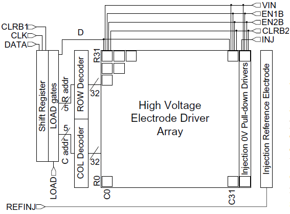
Figure 4. 32×32 Demonstration PFP chip architecture.
High Voltage Electrode Digital Driver Cell
Each electrode has an underlying driver cell as shown in Figure 5 consisting of two D latches (DL) in master-slave flip-flop operation that store the phase data, addressing logic controlled by a row (ROW) line and a column (COL) line, and a HV electrode driver. The HV electrode driver consists of a 2:1 mux controlled by the flip-flop outputs C and CB, a HV NMOS transistor connected to the high voltage supply VHH through a 5MΩ load resistor and an electrode connected to VOUT. The electrode output VOUT will be out-of-phase with the reference square wave VIN if C is logic low and in-phase if C is logic high. VIN sets the frequency of VOUT. An analog high-voltage electrode driver circuit has also been demonstrated for creating high voltage sinusoidal electrode excitations.
The electrode array’s next phase configuration is set by sequentially programming each site with the new phase data and then updating all phase outputs of the array simultaneously. A target driver is programmed by sending an 11-bit data sequence consisting of the 5-bit column address, 5-bit row address and 1-bit phase data into the DATA line of the SR controlled by CLK. After the data is set, addresses are passed to the decoders, and the phase data D is passed to the array cells by activating the gated output of the SR with the LOAD signal. The address enables only the target driver cell to accept the new phase data. When EN1B activates, the first DL of the target driver cell stores the new phase data from the D line and the memory is programmed. This entire programming sequence is repeated for each desired array cell. When all new data has been loaded, EN2B is activated, the second DL of each driver cell loads the new phase data and the output of the entire array is simultaneously updated with the new phase configuration.
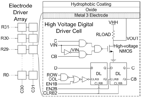
Figure 5. Electrode driver cell circuitry.
DEP-Assisted Droplet Injection Electronics
Fluid injectors are located to one side of the chip, their tips overlap the reference electrodes with their tips close to the last column of electrodes in the array (COL31). In the injection scheme, a DEP force creating the supplemental pressure needed to bring fluid from the injector tip onto the chip surface is generated by a potential difference between a grounded electrode in the last column of the array serving as the collecting electrode and the reference electrode exerting an arbitrary signal.
Any electrode in COL31 can be used for collection as each has a programmable injection driver, which pulls the output to a low DC voltage close to ground when activated. The injection driver circuitry is shown connected to its corresponding COL31 electrode in Figure 6 and is composed of a HV NMOS transistor, a flip-flop and addressing logic. Each injection driver shares the address of its adjacent driver cell but receives data from the INJ input. Programming an injection driver with a logic high INJ data turns on the HV NMOS transistor, which pulls the electrode output voltage near ground. The required signal can then be applied onto the injection reference electrode to induce droplet injection.
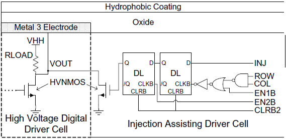
Figure 6. Injection driver connected to the adjacent electrode output in column 31.
Test Measurements and Results
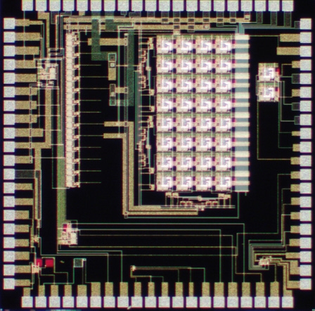
The die photo of the PFP chip is shown in Figure 7. A 1.0μm high-voltage, high-resistance, 1 poly, 3 metal, SOI CMOS fabrication technology is used. Figure 8 shows the electrode output at location (31,31) for two programming sequences. The top waveform shows the output square-wave change phases and then resetting to the initial phase during a 180-degree to 0-degree phase program and memory reset at 100V at 100Hz. The bottom waveform shows the output transitioning from a square-wave to ground state during a 180-degree to ground state program at 100V at 100Hz. Additional testing has shown operation of up to 200Hz at 100V and higher speeds are possible in the absence of a test probe.
Figure 9 shows a droplet of 180nL phosphate buffered saline in a 1-bromododecane medium being manipulated by the PFP chip coated with ~5μm of SU-8 topped with a monolayer of FluoroPel 1604 with microvinyl granules about 4μm across [1]. From t=0s, the droplet is moved downward until t=10s, to the right until t=42s, upward until t=88s, and to the left until t=115s.
Table 1 shows the specifications and measured performance of the PFP analyzer chip.
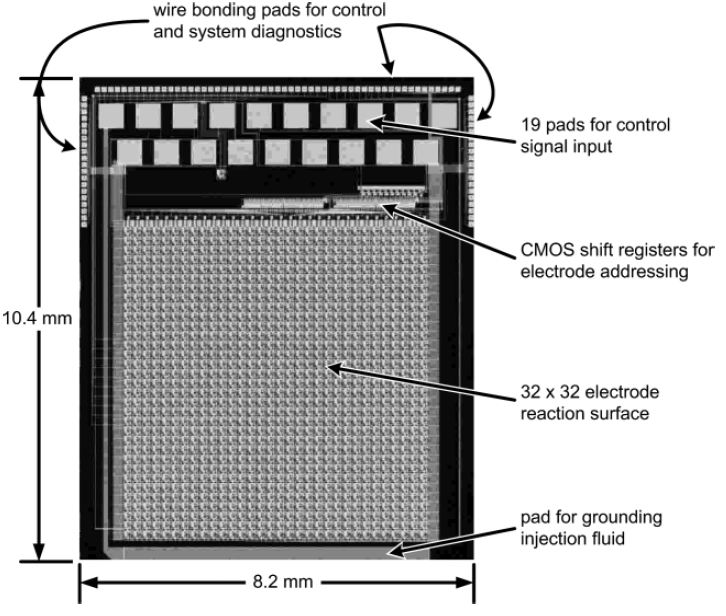
Figure 7. PFP chip photograph.
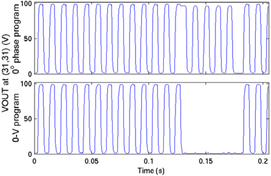
Figure 8. Electrode output at (31,31) for 0-degree phase program (top) and ground state program (bottom), both at VHH=100V, f=100Hz.
Conclusion
A VLSI chip that serves as the engine, generates the electrode excitations, for a Programmable Fluidic Processor has been demonstrated to precisely control the movement of droplets across its surface. This 10,377????m x 8210????m 32×32 demonstration chip is fabricated in a standard high-voltage 1????m SOI CMOS technology specified for 130V operation, and thus may be inexpensively mass-produced. Detection of droplet location and evaluation of droplet characteristics are presently done optically off-chip. On-chip electronic droplet location detection and electronic evaluation of droplet characteristics are under development. These developments may soon allow the deployment of inexpensive wristwatch-sized field chemical assay devices.
Acknowledgment
Research funded in part by DARPA contracts N66001-97-C-8608 from the Navy and DAAD19-00-1-0515 from the Army Research Office. The authors gratefully acknowledge contributions to this research by Harriet Lam, Alec Wong, and Peter Krulevitch.
References
[1] P. Gascoyne, J. Vykoukal, J. Schwartz, T. Anderson, D.Vykoukal, K.W. Current, C. McConaghy, F. Becker and C. Andrews, “Dielectrophoresis-based programmable fluidic processors,” Lab on a Chip, pp. 299-309, 2004.
[2] N. Manaresi, A. Romani, G. Medoro, L. Altomare, A. Leonardi, M. Tartagni, and R. Guerrieri, “A CMOS Chip for Individual Cell Manipulation and Detection,” IEEE JSSC, Vol. 38, No. 12, pp. 2297-2305, Dec 03
[3] J.R. Keilman, G.A. Jullien and K.V.I.S Kaler, “A SoC bio-analysis platform for real-time biological cell analysis-on-a-chip,” Proceedings of The 3rd IEEE International Workshop on System-on-Chip for Real-Time Applications, IEEE, 2003.
[4] Y. Li and K.V.I.S. Kaler, “DEP based cell separation utilizing planar microelectrode array,” 2002 Annual Report Conference on Electrical Insulation and Dielectric Phenomena, IEEE, 2002.
[5] P Gascoyne, X Wang, Y Huang, F Becker, “Dielectrophoretic separation of cancer cells from blood,” IEEE Trans Industry Applications, V 33, n 3, pp. 670 –678, May-June 1997.
[6] X.-B. Wang, Y. Huang, P. R. C. Gascoyne, and F. F. Becker, IEEE Trans Ind Apps, 1997, 33(3), pp. 660-669.
[7] J. Vykoukal, J. Schwartz, F. Becker, P. Gascoyne, “A programmable dielectrophoretic fluid processor for droplet-based chemistry,” Micro Total Analysis Systems 2001, pp. 72-74, 2001.

